-
Customer Service QQ
3297421414
-
Phone
Monday to Saturday 9:30 - 22:00
Phone : 18682486380
18126541905 -
Official WeChat
 Scan the official WeChat QR code for an instant quote
Jiechi Electronics Co., Ltd.
100% quality | A global multi-service platform for electronic components
Customer Service QQ
3297421414
Phone
Monday to Saturday 9:30 - 22:00
Phone : 18682486380
18126541905
Official WeChat
Scan the official WeChat QR code for an instant quote2021-08-16 Views:0
ADL6317 is a transmit variable gain amplifier (VGA) that provides an interface from a radio frequency digital-to-analog converter (RF DAC), transceiver, and system-on-chip (SoC) to the power amplifier. Integrated baluns and hybrid couplers enable high-performance RF functionality from 1500 MHz to 3000 MHz.
To optimize performance and power levels, the ADL6317 includes a voltage variable attenuator (VVA), high linearity amplifier, and a digital step attenuator (DSA). All devices integrated in the ADL6317 are programmable through the 4-wire serial port interface (SPI).
ADL6317 is manufactured using advanced silicon germanium (SiGe), bipolar complementary metal oxide semiconductor (BiCMOS) process.
ADL6317 Main features: The
VGA pass-to-power amplifier interface for RF DACs, transceivers and SoCs
RF output frequency range: 1500 MHz to 3000 MHz
Internal balun with biased T-tube provides RF DAC output
Integrated VVA attenuation range with on-chip DAC: 20.5 dB
2-stage high linearity amplifier
RF DSA attenuation range: 15.5 dB, 0.5 dB step resolution
50 Ω differential input and 50 Ω single-ended output
realizes bidirectional high power conversion through 4-wire SPI
single 5 V power supply is fully programmable. The communication between the
38-terminal, 10.5 mm × 5.5 mm LGA
ADL6317 Application:
Application of 2G/3G/4G/LTE in FDD/TDD broadband communication system
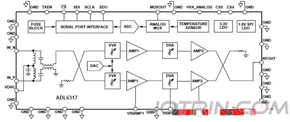
Figure 1. ADL6317 function
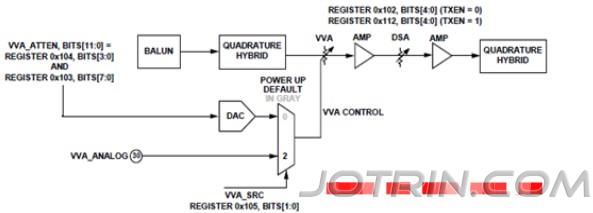
Figure 2. ADL6317 RF signal chain
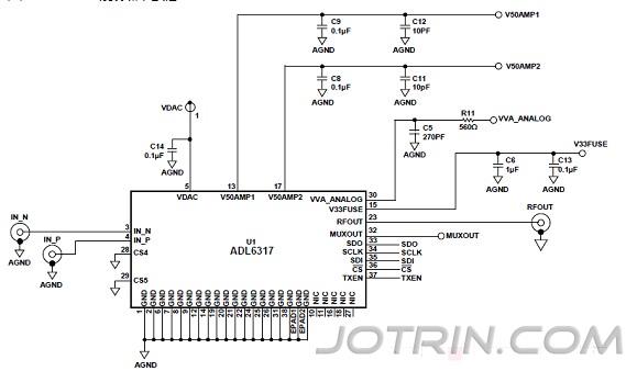
Figure 3. ADL6317 basic connection
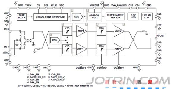
Figure 4. ADL6317 signal limited enable alone
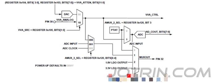
Figure 5. ADL6317 auxiliary multiplexer
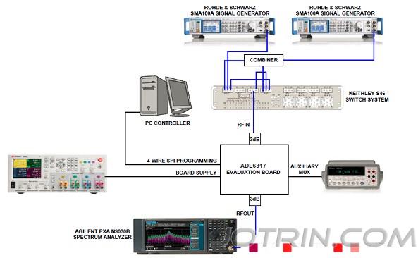
RF establishment diagram 6. ADL6317 general characteristics diagram
ADL6317 Evaluation Board
EvaluaTIng TxVGAs for Use with DACs and Transceivers
ADL6317 is a transmitter variable gain amplifier (VGA) that can provide from radio frequency (RF) Digital-to-analog converters (DACs), transceivers, and system-on-chip (SoC) to power amplifier (PA) interfaces. Integrated baluns and hybrid couplers allow high-performance RF functionality in the 1.5 GHz to 3.0 GHz frequency range. The
To optimize performance and power levels, the ADL6317 includes a voltage variable attenuator (VVA), high linearity amplifier, and a digital step attenuator (DSA). Devices integrated into the ADL6317 are programmable through the 4-wire serial port interface (SPI).
This user's guide describes the ADL6317 evaluation board and software. For complete details, please refer to the ADL6317 data sheet, which must be consulted in conjunction with this user guide when using
Evaluation Committee. ADL6317 evaluation board
Made of FR-370HR, Rogers 4350B four layers.
ADL6317 Evaluation Board Main Features: ADL6317 Evaluation Board is powered by a SDP-S board 5.0 V single power supply