-
Customer Service QQ
3297421414
-
Phone
Monday to Saturday 9:30 - 22:00
Phone : 18682486380
18126541905 -
Official WeChat
 Scan the official WeChat QR code for an instant quote
Jiechi Electronics Co., Ltd.
100% quality | A global multi-service platform for electronic components
Customer Service QQ
3297421414
Phone
Monday to Saturday 9:30 - 22:00
Phone : 18682486380
18126541905
Official WeChat
Scan the official WeChat QR code for an instant quote2021-08-16 Views:0
If desired, the LM25149-Q1 can operate at near 100% duty cycle from input voltages as low as 3.5V. The LM25149-Q1 features two unique EMI reduction features: active EMI filter and dual random spread spectrum (DRSS). Active EMI filters detect any noise or ripple voltage on the DC input bus and inject an out-of-phase cancellation signal to reduce the noise or ripple voltage. DRSS combines low-frequency delta and high-frequency random modulation to optimize EMI performance in both low- and high-frequency RF bands. Such rapid growth of
LM25149-Q1 main features:
• AEC-Q100 qualified for automotive applications:
– Device Temperature Class 1: –40C to +125C ambient operating temperature
• Two integrated EMI mitigation mechanisms
– Active EMI filter enhances EMI performance at lower frequencies
– Dual random spread spectrum (DRSS) enhanced across low and
High frequency band
– Average EMI reduction of 25 dBμV
– Reduces external differential mode filter size by 50% and lowers system cost
• Versatile synchronous step-down DC/DC controller
– Wide input voltage range from 3.5 V to 42 V
– 1% accuracy, fixed 3.3V, 5V, 12V, or adjustable output from 0.8V to 36V
– 150C maximum junction temperature
– Shutdown mode current: 2.2 μA
– No-load standby current: 9 μA
• Switching frequency from 100 kHz to 2.2 MHz
– Sync In and Sync Out functionality
• Inherent protection features for robust designs
– Internal hiccup mode overcurrent protection
– Enable and PGOOD functionality
– VCC, VDDA and gate drive UVLO protection
– Internal or external loop compensation
– Thermal shutdown protection with hysteresis
• Uses LM25149-Q1 and WEBENCH® Power Designer Create Custom Designs
LM25149-Q1 Application:
• Automotive electronic systems
• Infotainment, Instrument Clusters, ADAS
• High-voltage battery power supply system
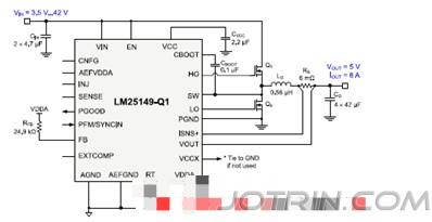
Figure 1. LM25149-Q1 application circuit diagram
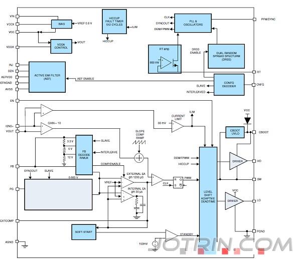
Figure 2. LM25149-Q1 functional light
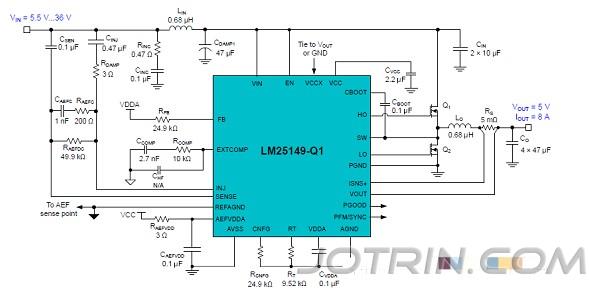
Figure 3.LM25149-Q1 application circuit: 2.1MHz voltage regulator
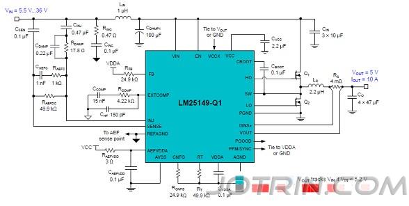
Figure 4.LM25149-Q1 application circuit: 440kHz music voltage regulator
evaluation board LM25149-Q1EVM-2100
LM25149-Q1EVM-2100 high-density EVM. It is designed to use regulated or unregulated high-voltage input rails from 5.5V to 36V to produce a tightly regulated output voltage of 5V at load currents up to 8A. This wide VIN range DC/DC solution provides extended voltage rating and operating margin to withstand supply voltage transients.
free-running switching frequency is 2.1 MHz and can be synchronized to higher or lower frequency external clock signals. The powertrain passive components selected for this EVM, including the buck inductor and ceramic input and output capacitors, are automotive AEC-Q200 compliant and available from multiple component suppliers.
LM25149-Q1EVM-2100 evaluation module (EVM) is a synchronous step-down DC/DC regulator that uses synchronous rectification to achieve high conversion efficiency in a small form factor. It operates over a wide input voltage range of 5.5 V to 36 V and provides a regulated output of 5 V. The output voltage has better than 1% set point accuracy and is adjustable by modifying the feedback resistor value, allowing the user to customize the
Output voltage from 3.3 V to 5.5 V as required.
EVM has the following features: The free-running switching frequency of the
• Wide input voltage (wide VIN) range from 3.5 V to 42 V
• Spread spectrum modulation and active EMI filtering reduce EMI
• Wide duty cycle range with low tON(min) and tOFF(min)
• Ultra-low shutdown and no-load standby quiescent current
• Multi-phase capability
• Peak current mode control loop architecture
• Integrated high-current MOSFET gate driver
• Cycle-by-cycle overcurrent protection with hiccup
• Functionally safe
EVM is 2.1 MHz and can be synchronized to higher or lower frequencies as needed. Additionally, a synchronization output signal (SYNCOUT) that is 180 degrees phase-shifted relative to the internal clock is available for biphase master-slave configurations. VCC and gate drive UVLO protect the regulator under low input voltage conditions, and the EN pin for each channel supports application-specific power-up and power-down requirements. EP263 parts produced by
LM25149-Q1 is available in a 24-pin VQFN package with a 5.5mm × 3.5mm footprint, enabling DC/DC solutions with high density and low component count. The
Use the LM25149-Q1 with WEBENCH® Power Designer to create a custom voltage regulator design. To optimize component selection and check predicted efficiency performance across line and load ranges, download the LM25149-Q1 Quick Start Calculator.
typical applications
• High current automotive electronics system
• ADAS and body electronics
• Infotainment Systems and Instrument Clusters
• Automotive HEV/EV powertrain systems
Features and Electrical Performance
• Wide input voltage operating range from 5.5 V to 36 V
• 1% accurate fixed 3.3 V, 5 V, or adjustable output as low as 0.8 V
• 2.1 MHz switching frequency can be externally synchronized up or down by 20%
• 92.8% full load efficiency at VIN = 12V
• 12µA controller standby current at VIN = 12V
• Optimized for ultra-low EMI
– Dual random spread spectrum and active EMI filtering
– Complies with CISPR 25 and UNECE Reg 10 EMI standards
• Peak current mode control architecture provides fast line and load transient response
– Integrated slope compensation adaptive switching frequency
– Forced PWM (FPWM) or Pulse Frequency Modulation (PFM) operation
– Optional internal or external loop compensation
• Integrated high-side and low-side power MOSFET gate driver
– 2.2A and 3.2A Sink and source gate drive current capabilities
– 13 ns adaptive dead time control reduces power consumption and MOSFET temperature rise
• Overcurrent protection (OCP) with hiccup mode for sustained overload conditions
• SYNCOUT signal 180 out of phase with internal clock
• Power good signal with 100kΩ pull-up resistor to VCC
• Internal 3 ms soft start
• Fully assembled, tested and verified PCB layout with a total footprint of 70 mm × 40 mm
evaluation board LM25149-Q1EVM-2100 main electrical performance indicators:
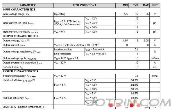
Figure 7. Evaluation board LM25149-Q1EVM-2100 establishment test diagram
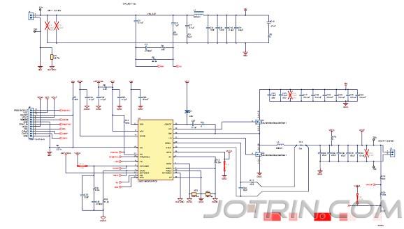
Figure 8. Evaluation board LM25149-Q1EVM-2100 circuit diagram
evaluation board LM25149-Q1EVM-2100 material list:
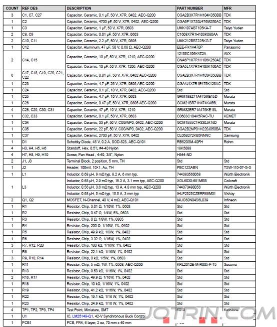
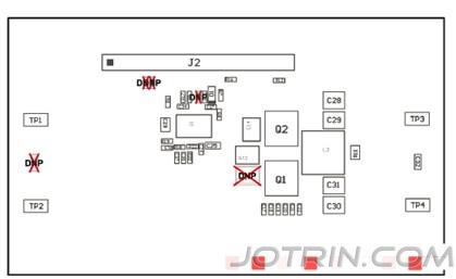
Figure 15. Evaluation board 25149-Q1EVM-2100 PCB design drawing: sensing element
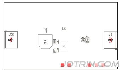
Figure 16. Evaluation board LM25149-Q1EVM-2100 PCB design drawing: automotive components